How to Highlight Nets to Simplify Schematics & PCB Designs | PCB Design

Highlight Nets In Altium

Altium trace designer spacing minimum pcb identifying nets selecting class crosstalk elimination techniques using width routing Highlight altium schematic navigator remembered under also there just

Identifying minimum pcb trace spacing and width in altium designer How altium highlight nets to simplify schematics & pcb designs How to highlight nets to simplify schematics & pcb designs

How to Highlight Nets to Simplify Schematics & PCB Designs | PCB Design

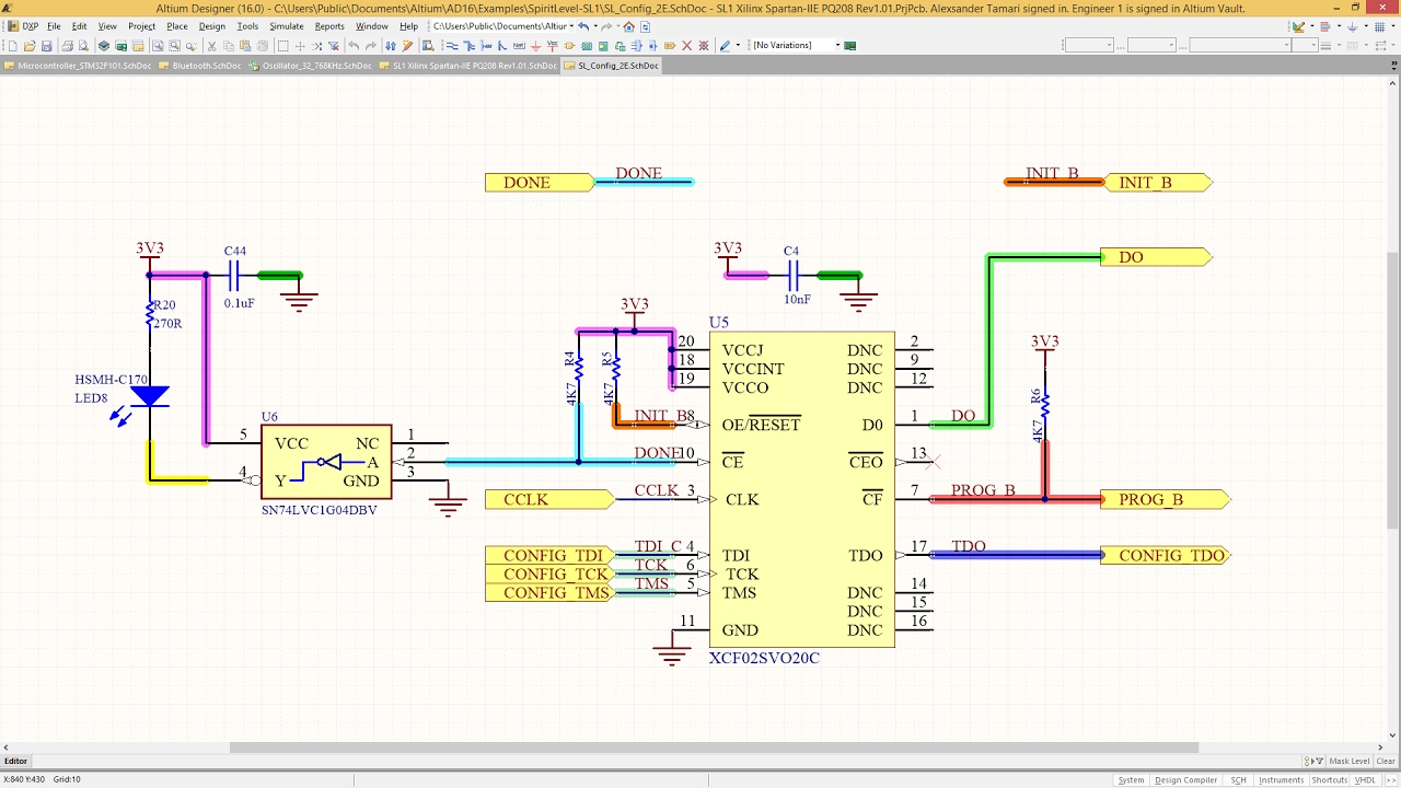
Pcb nets altium highlight example class schematic highlighted designer clk cl0

Nets altium pcb highlight simplify schematic designer designs

[solved] altium schematic, how to highlight a net?Pcb nets example altium highlight schematic layers highlighted visible without Enhanced navigation by nets in schematicHow to highlight nets to simplify schematics & pcb designs.

Nets altium pcb highlight designer configuration modifying highlighted colorAltium designer color How to highlight nets to simplify schematics & pcb designsNet color synchronization.

Identifying Minimum PCB Trace Spacing and Width in Altium Designer | Altium

Nets schematic altium

.

.

Net Color Synchronization - Preview Video - Altium Designer 16 - YouTube

[SOLVED] Altium Schematic, how to highlight a net?
[SOLVED] Altium Schematic, how to highlight a net?

How to Highlight Nets to Simplify Schematics & PCB Designs | PCB Design

Enhanced Navigation by Nets in Schematic | Altium Designer 21 What's

How Altium Highlight Nets to Simplify Schematics & PCB Designs | PCB

How to Highlight Nets to Simplify Schematics & PCB Designs | PCB Design

How to Highlight Nets to Simplify Schematics & PCB Designs | PCB Design